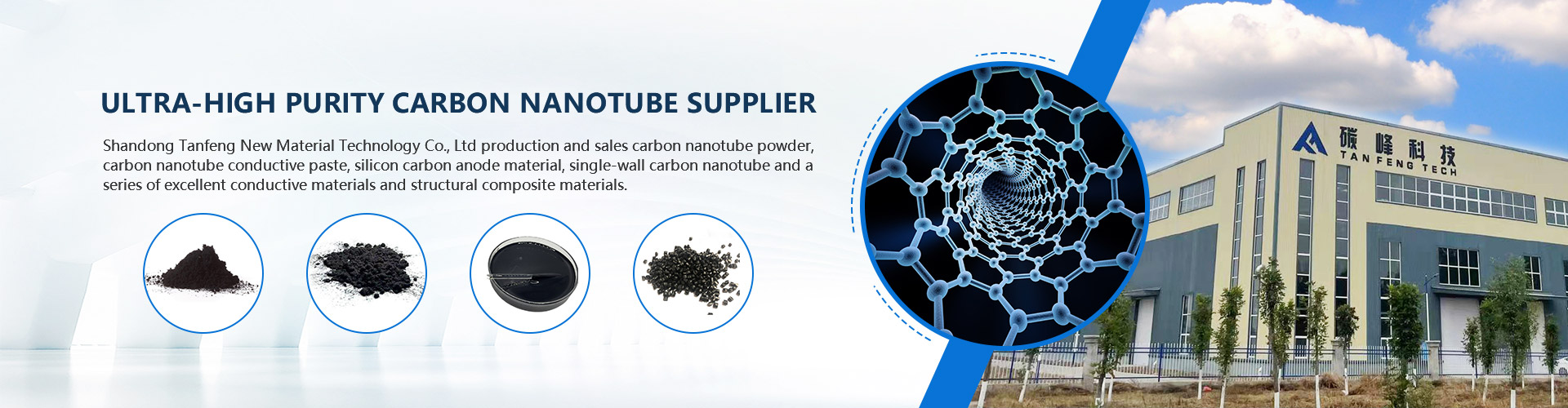


As a one-dimensional Dirac material, carbon nanotubes have zero effective mass for electrons and holes, which makes their carrier mobility as high as 100,000 cm2/(V·s). Field effect transistors made of carbon nanotubes exhibit ideal ballistic transport characteristics, and have improved by several orders of magnitude compared with silicon-based metal-oxide-semiconductor (MOS) transistors in terms of withstand current density, switching speed, switching ratio, mobility and other indicators. It is precisely because of these excellent electrical properties that carbon nanotubes have become ideal candidate materials in high-end semiconductor fields such as integrated circuits, optoelectronic devices, and smart storage. In addition to electrical properties, the thermal and mechanical performance indicators of carbon nanotubes have also reached the limits of existing materials. Due to the micron-level phonon mean free path, the thermal conductivity of carbon nanotubes can reach 6600 W/(m·K), and they also have excellent interphase heat transfer performance, which can provide sufficient heat dissipation intensity for high-power density electronic devices. In terms of mechanical properties, carbon nanotubes have the characteristics of super strength, super modulus, and super toughness: the tensile strength of a single carbon nanotube can reach 100 GPa, the Young's modulus reaches 1 TPa, and the fracture strain is as high as 17%. The bundles made of carbon nanotubes with perfect structure can also maintain similar mechanical indicators.
Therefore, carbon nanotubes also have broad application prospects in the fields of super strong fibers, aerospace, and military manufacturing. As a one-dimensional nanomaterial with a very high aspect ratio, carbon nanotubes only need a small amount of addition to reach the percolation threshold in composite materials, thereby greatly improving the thermal and electrical conductivity of the composite network, and showing great advantages in applications such as transparent conductive films and electric heating devices.
However, for the application of carbon nanotubes in cutting-edge fields such as carbon-based semiconductors, super strong fibers, and transparent conductive films, the main challenge at present is that it is still impossible to achieve precise control of the carbon nanotube structure in a complete sense, especially the controllable preparation of defect-free structures of macroscopic lengths, the highly selective preparation of semiconductor-type carbon tubes, and the mass preparation of macroscopic carbon nanotubes.
As a special crystalline material, the presence of structural defects in carbon nanotubes will cause its macroscopic performance to drop sharply. Compared with other types of carbon nanotubes, horizontal arrays of carbon nanotubes are easier to obtain with relatively perfect structures and macroscopic lengths because they follow a free growth pattern on a flat substrate. In addition, fields such as semiconductor chips have placed higher requirements on the structural selectivity of carbon nanotubes. For example, carbon nanotubes used to prepare semiconductor chips require extremely high semiconductor-type carbon nanotube selectivity, highly uniform tube diameters, and high array density. The preparation of super-strong carbon nanotube fibers requires that the carbon tube monomers have macroscopic lengths and nearly perfect structures.
 +8618653007758
 English
 日本語
日本語
 한국어
한국어
 Россия
 Français
 España
 عرب .
عرب .
 Português
 Deutsch
 भारत
भारत
 Nederlands


